
Japan to cut off the supply of advanced packaging equipment to China starting August 1st.
On August 1, Japan's third round of new export controls on semiconductor equipment officially came into effect, including core equipment for the entire advanced packaging chain in a list of
时政
(
twitter.com
)
Japan to cut off the supply of advanced packaging equipment to China starting August 1st.
On August 1, Japan's third round of new export controls on semiconductor equipment officially came into effect, including core equipment for the entire advanced packaging chain in a list of strict controls. The regulations adopt a case-by-case approval model, and with a long approval cycle and an extremely high rejection rate, they effectively cut off the supply to the domestic market.
This marks the third major upgrade to Japan's semiconductor export controls on China, focusing on addressing the shortcomings previously addressed primarily in front-end wafer manufacturing equipment and bringing core equipment across the entire advanced packaging chain under strict control.
The first round (July 2023): Japan will include 23 categories of advanced semiconductor manufacturing equipment under export controls, including cleaning, deposition, heat treatment, photolithography, etching, and inspection equipment, mainly targeting equipment capable of producing logic chips at 14nm and below.
Second round (2025): Further tighten and expand the control list, strengthen control over photoresists, materials and catch-all supplements.
The third round (announced in May 2026, effective August 1): On May 29, 2026, the Ministry of Economy, Trade and Industry (METI) of Japan revised the relevant list of the Foreign Exchange and Foreign Trade Act, and for the first time included a complete set of back-end packaging and testing equipment for advanced packaging (Chiplet/3D stacking/CoWoS/TSV) in the export control list.
The newly added key controlled items (approximately 20 categories, with core components related to back-end packaging and testing) include: high-end die bonders, ultra-thin wafer thinning/grinding machines, laser cutting/hidden dicing machines such as DISCO, TSV (Through Silicon Via) equipment, bump fabrication/micro-bump plating equipment, high-precision chip sorting machines, hybrid bonding machines, flexible bonding equipment, and related high-end testing equipment.
Previous sanctions imposed by the US, Japan, and the Netherlands mostly focused on front-end wafer manufacturing equipment such as lithography and etching machines. This round of restrictions, however, has pinpointed China's weakness: advanced packaging equipment.
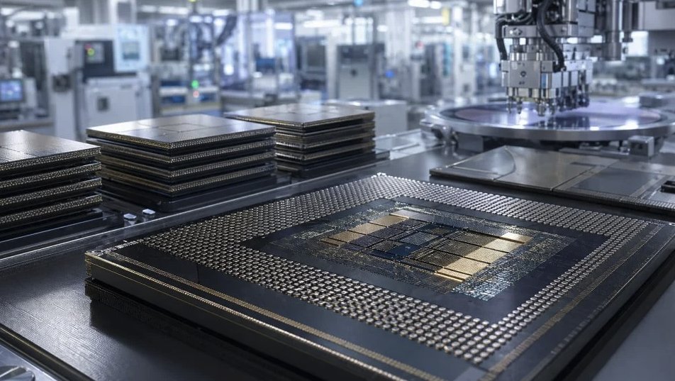
Today, advanced chip manufacturing processes are approaching physical limits. To produce high-performance computing chips and HBM high-speed memory chips at low cost, chiplets and 3D stacking packaging are the most feasible breakthrough paths. Ultra-thin wafer thinning machines, laser slicing machines, high-end die bonders, and TSV silicon via equipment are the hardware foundation of this route, and the market has long been monopolized by companies such as Japan's DISCO.
According to the new regulations, all new orders for this type of equipment to China will require separate export licenses, with an approval cycle of 3-6 months. The rejection rate for applications for advanced process equipment is close to 80%. Existing orders signed before August 1st will only have a one-month transition period for fulfillment. After the transition period ends, new machine procurement and original manufacturer maintenance services will be completely discontinued.
点击图片查看原图

